Japanese
  English
  Chinese
  Spanish
  Portuguese
  German

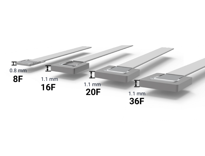
大きなメリット、小さなフットプリント
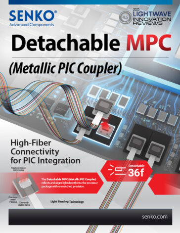
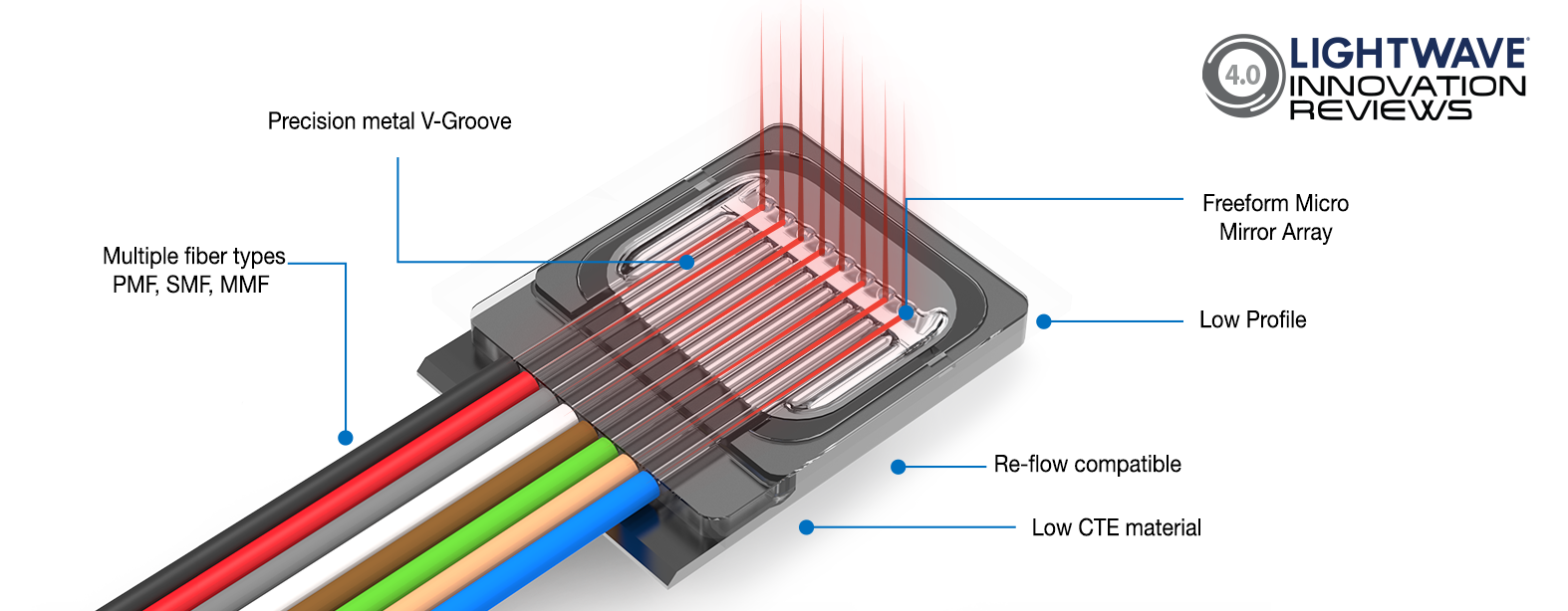
MPCは、高反射率の金属製光学ミラーを利用し、光を正確に形作り、次のように誘導する。 およびPIC(フォトニック集積回路)からのものである。MPCは、EDGEと SURFACEカップリングには、PERMANENTとDETACHABLEの両方のバリエーションがあります。により製造されます。 独自のスタンピングプロセスにより、MPCはコスト効率の高い大量生産への道を開く。 を製造している。

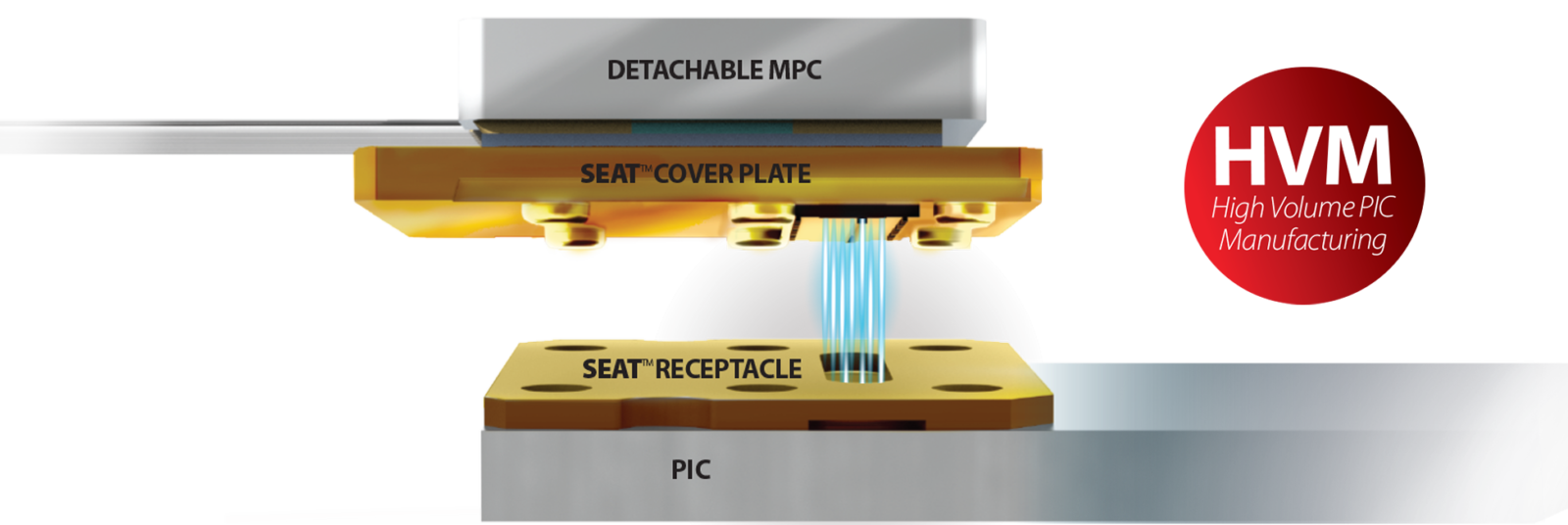
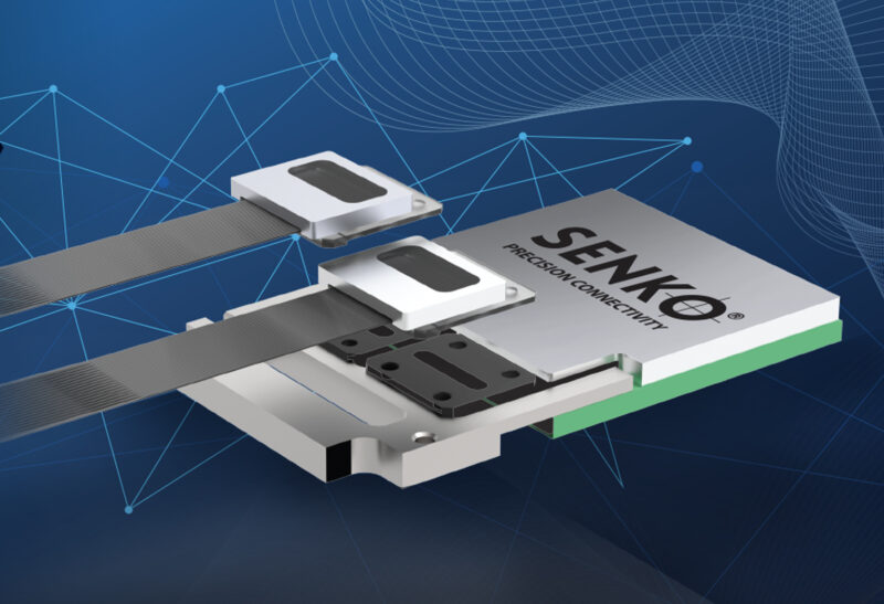
SEAT™ Technology Enables Co-Packaged Optics at Scale
Wafer-level photonics is transforming the future of optical networks, but only when testing and alignment can keep pace. By integrating SEAT™ and MPC with GlobalFoundries’ silicon photonics process, fine mechanical alignment, detachability, and repeatable optical coupling are possible from wafer-level testing through packaged photonic engines.
PICカップリングの実用化
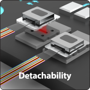
着脱性
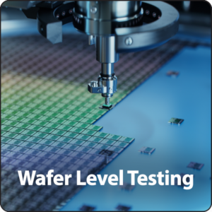
ウェハー・レベル・テスト
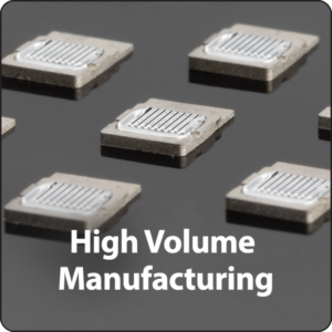
大量生産
Enabling the Photonics Ecosystem
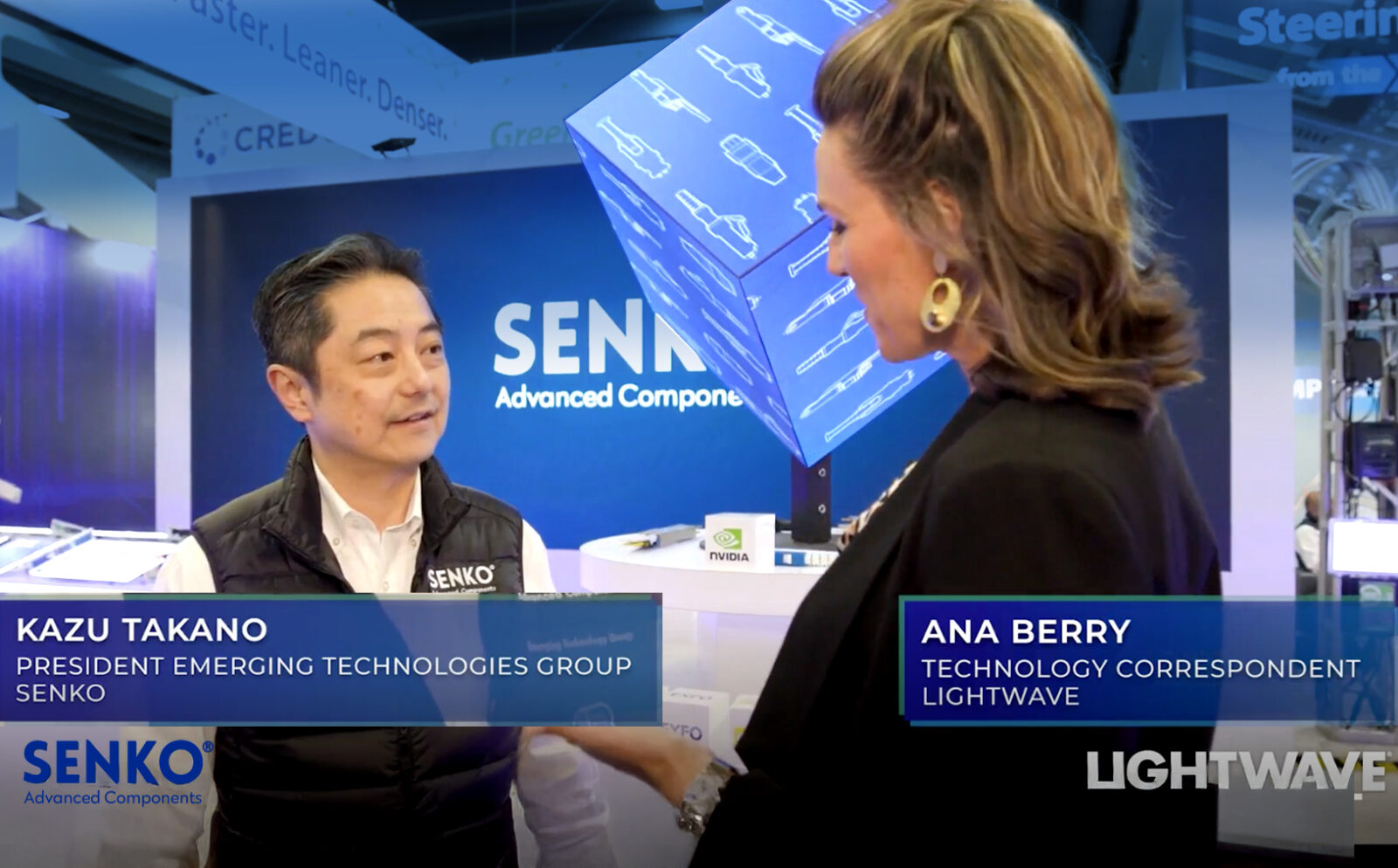
Eric Snow, Fellow, Photonic Test Platforms at GlobalFoundries, discusses the shift of photonic integrated circuits from lab environments into high-volume manufacturing ecosystems. Detachable optical interfaces are emerging as an enabler across the Co-Packaged Optics (CPO) value chain, improving yield, manufacturability, and interoperability across the AI ecosystem.

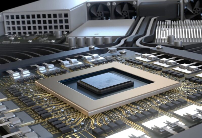
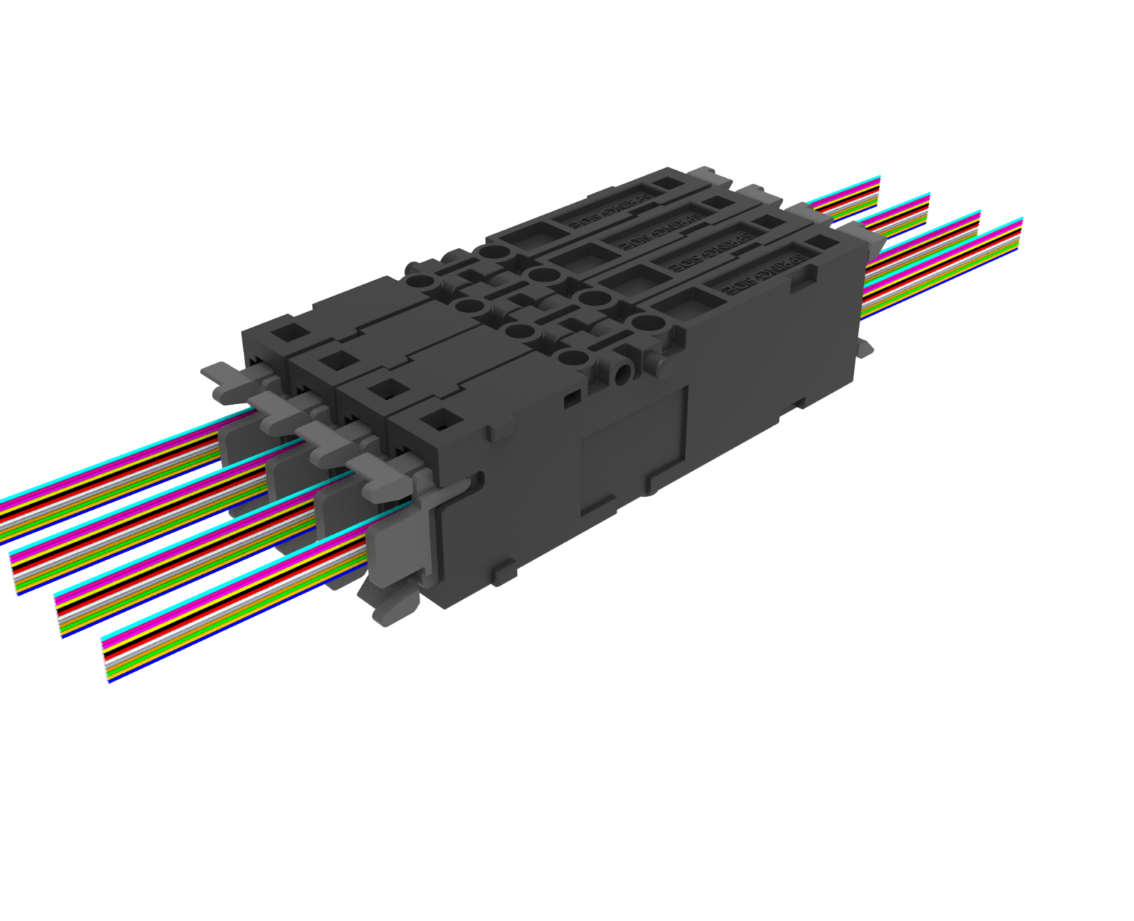
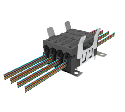
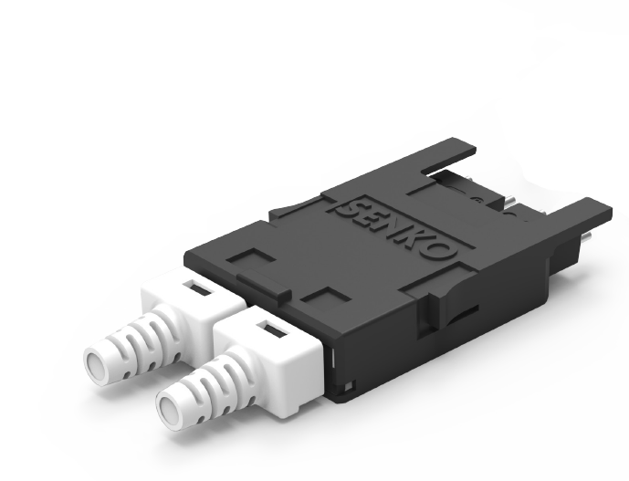
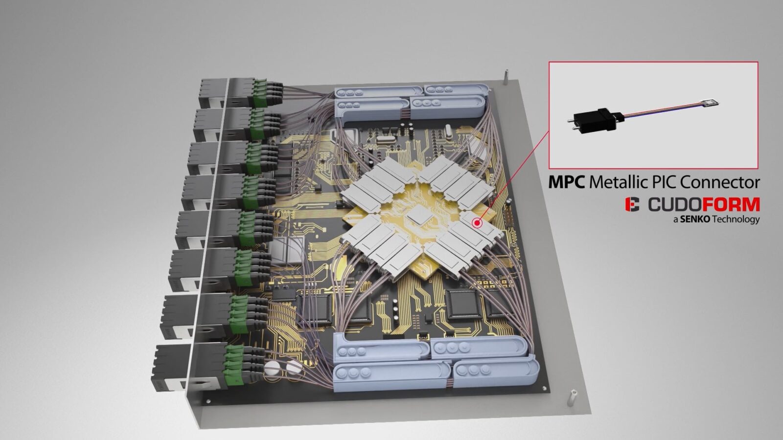
MPCは世界最小の金属製PICコネクターです。その薄型で着脱可能な設計は、混雑したCPOスイッチ環境内での最適なスペース利用を容易にします。
MPCアプリケーション
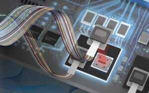
CPOスイッチ
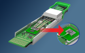
プラグ可能トランシーバー
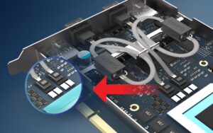
PCIEカード
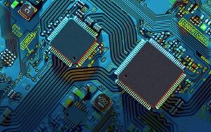
新たなテクノロジー
関連製品
PICカップリング
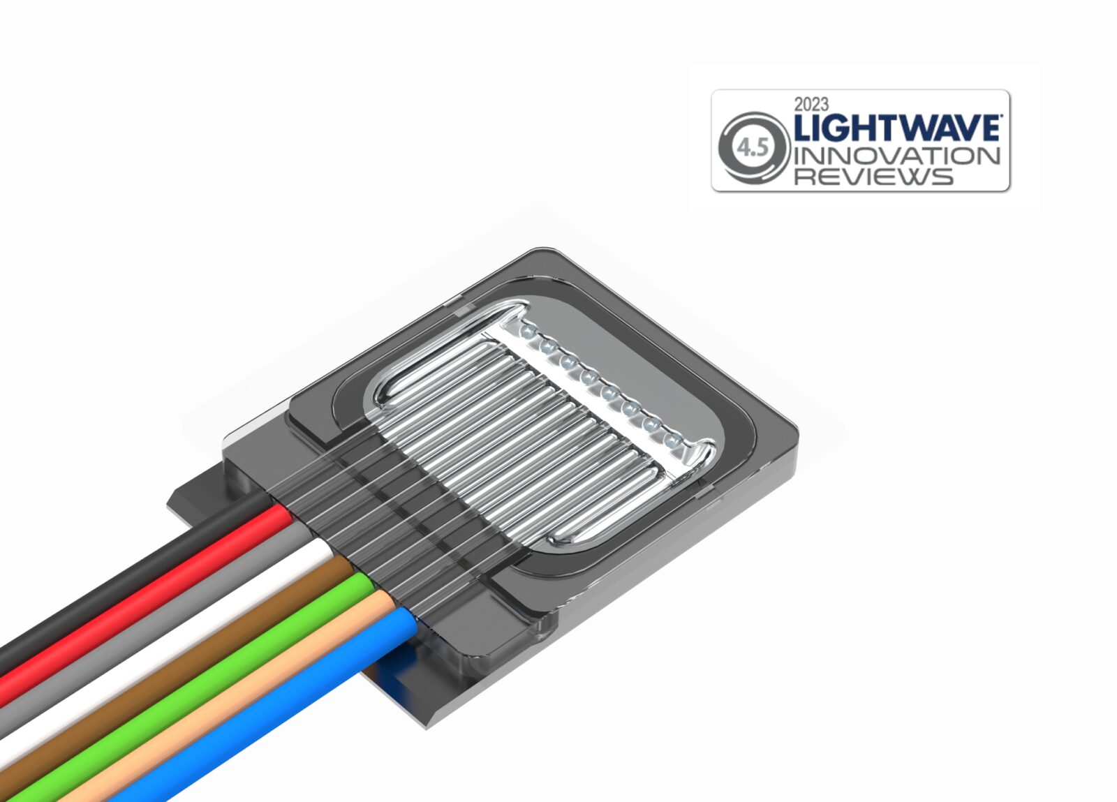
メタリックPICコネクターは、金属製の光ベンチをプレス加工して作られています。
MPC - メタリックPICコネクタ
製品を見るPICカップリング
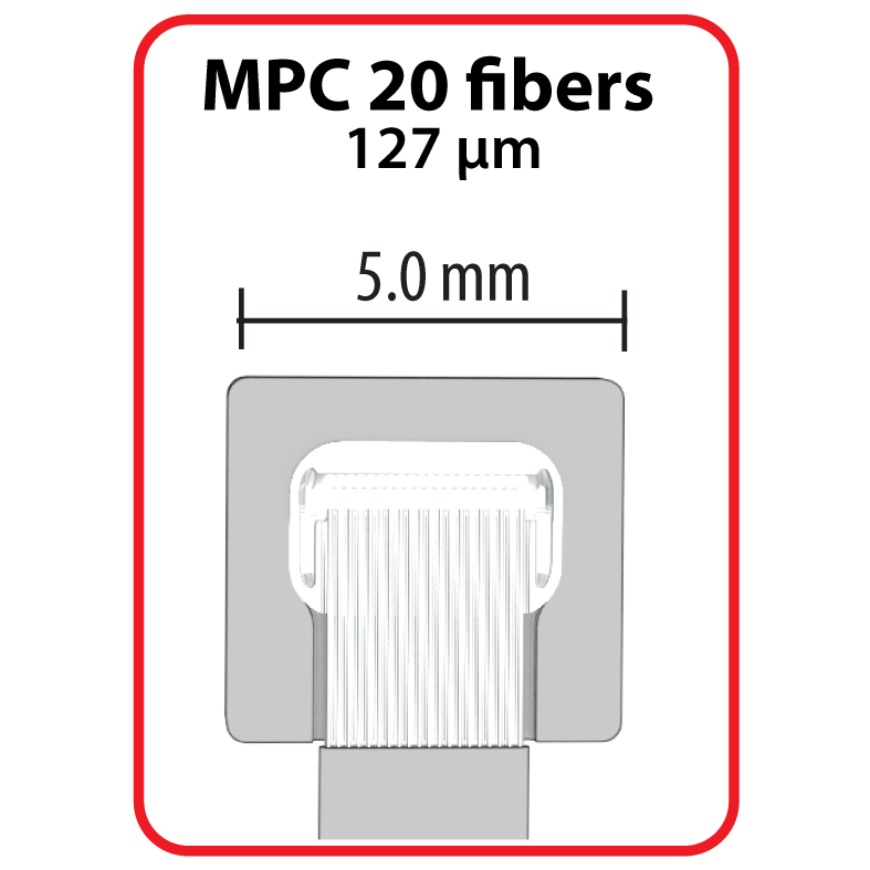
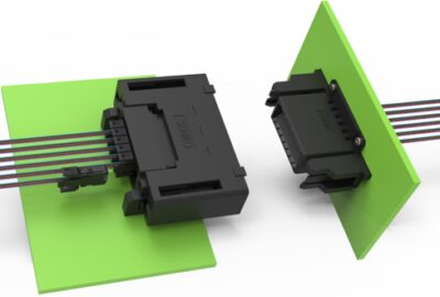
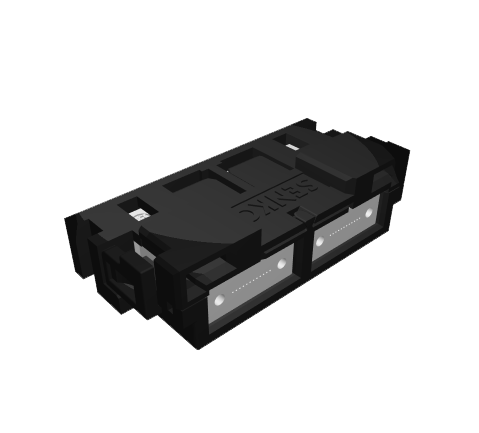
MPC20は、業界の重要な課題に対処するために設計された革新的なソリューションです。
MPC 20
製品を見る